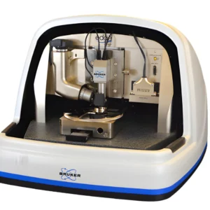
Description
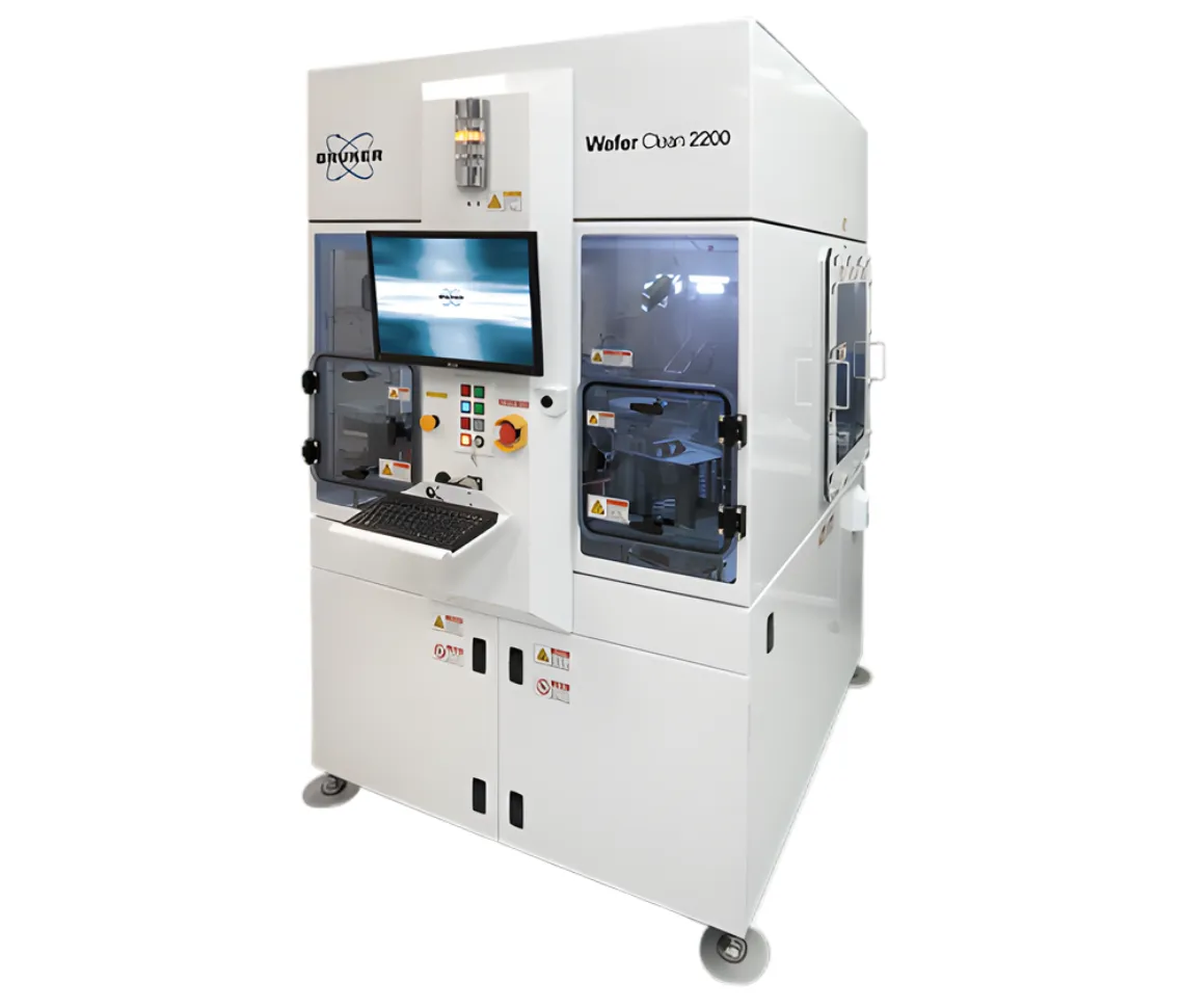
The Bruker Wafer Clean 2200 is a cryogenic dry CO₂ wafer cleaning system engineered to remove particulate contamination and thin organic residues from silicon, compound semiconductor, MEMS, and thin film head substrates. It uses a unique CO₂ snow cleaning technology that is fast, non-damaging, and completely dry, offering substantial advantages over traditional wet or lasma cleaning techniques.
The process is environmentally safe, solvent-free, and generates zero hazardous waste. The system is fully automated and optimized for high-volume semiconductor production, with more than 100 units operating 24/7 worldwide. Its raster scan movement and precision control enable global and local cleaning with high efficiency, achieving particulate removal down to 120 nm and eliminating ion beam etch veil and fence artifacts.
The Wafer Clean 2200 is widely used for photoresist veil removal, MEMS device cleaning, and general cryogenic CO₂ cleaning applications. Its capabilities help improve device reliability and wafer-level yield.
Wafer Clean 2200 — Summary Table
| Category | Key Details |
|---|---|
| System Type | Cryogenic dry CO₂ wafer cleaning system |
| Cleaning Method | CO₂ snow cleaning; all-dry, non-damaging, solvent-free |
| Key Functions | Removes particulates and thin organic residues from silicon, compound semiconductor, MEMS, and thin film substrates |
| Throughput | 25 wafers per hour (WPH) |
| Motion System | Raster scan movement for uniform coverage |
| Cleaning Modes | Supports global and local cleaning |
| Yield Benefits | Improves wafer-level yield by removing particles and residues |
| Cleaning Resolution | Effective particle removal down to 120 nm |
| Artifact Removal | Removes ion beam etch (IBE) veil and fence residues |
| Environmental Benefits | Environmentally safe, solvent-free, zero hazardous waste |
| Production Readiness | Fully automated; over 100 systems active in 24/7 high-volume production |
| Core Applications | Photoresist veil removal, MEMS device cleaning, cryogenic CO₂ cleaning processes |
| Ideal Users | Semiconductor fabs, MEMS manufacturers, thin-film device producers |