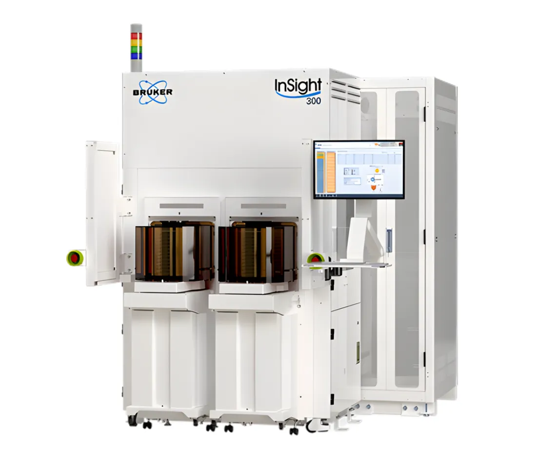
Description
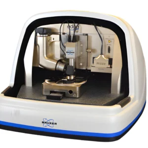
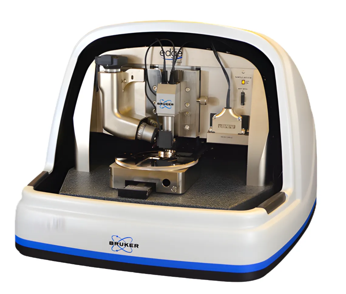
The Bruker InSight 300 is a high-throughput, highly accurate automated AFM platform designed for inline semiconductor metrology.
Built on more than 25 years of AFM innovation, it delivers exceptional resolution, stability, and reliability at a low total cost
of ownership. Bruker’s expertise in automated AFM (AAFM) ensures robust performance for advanced-node device manufacturing.
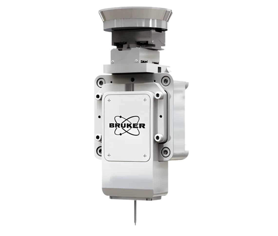
Its capabilities include specialized probes, application-specific operating modes, fully automated tip handling, continuous
performance verification, high-quality integrated optics, and a modern GUI. The system supports key metrology applications such as
roughness, depth, sidewall profiling, defect review, surface profiling, and hybrid bonding.
Bruker’s global service organization, strategically positioned parts depots, and comprehensive support programs ensure maximum uptime
and consistent process control in high-volume manufacturing environments.
InSight 300 — Summary Table
| Category | Key Details |
|---|---|
| Purpose | High-throughput, accurate, inline AFM metrology for semiconductor manufacturing |
| Core Strengths | High stability, accuracy, repeatability, low cost of ownership, long-term reliability |
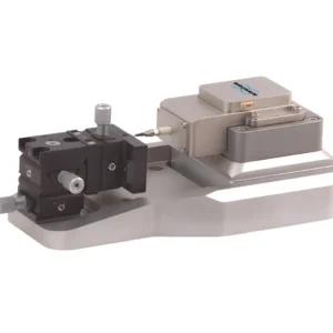
| Specialized Probes | Application-dedicated probe designs; Bruker manufactures its own probes; optimized for sidewalls, high-aspect-ratio features, and diverse materials |
| Application-Specific Modes | TrueSense® (roughness), CDMode (sidewall angle/roughness), DTMode (deep trench/via depth), Profiling (surface mapping) |
| Automatic Tip Management | TipX automation; automatic loading & qualification; vacuum-held probes; 25-probe cassette; reduces probe cost |
| Performance Verification | Sub-nanometer stability (<±1 nm); high linearity; 18 µm Z range; 105 µm² scan area; long-range profiling stage |
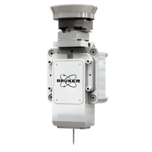
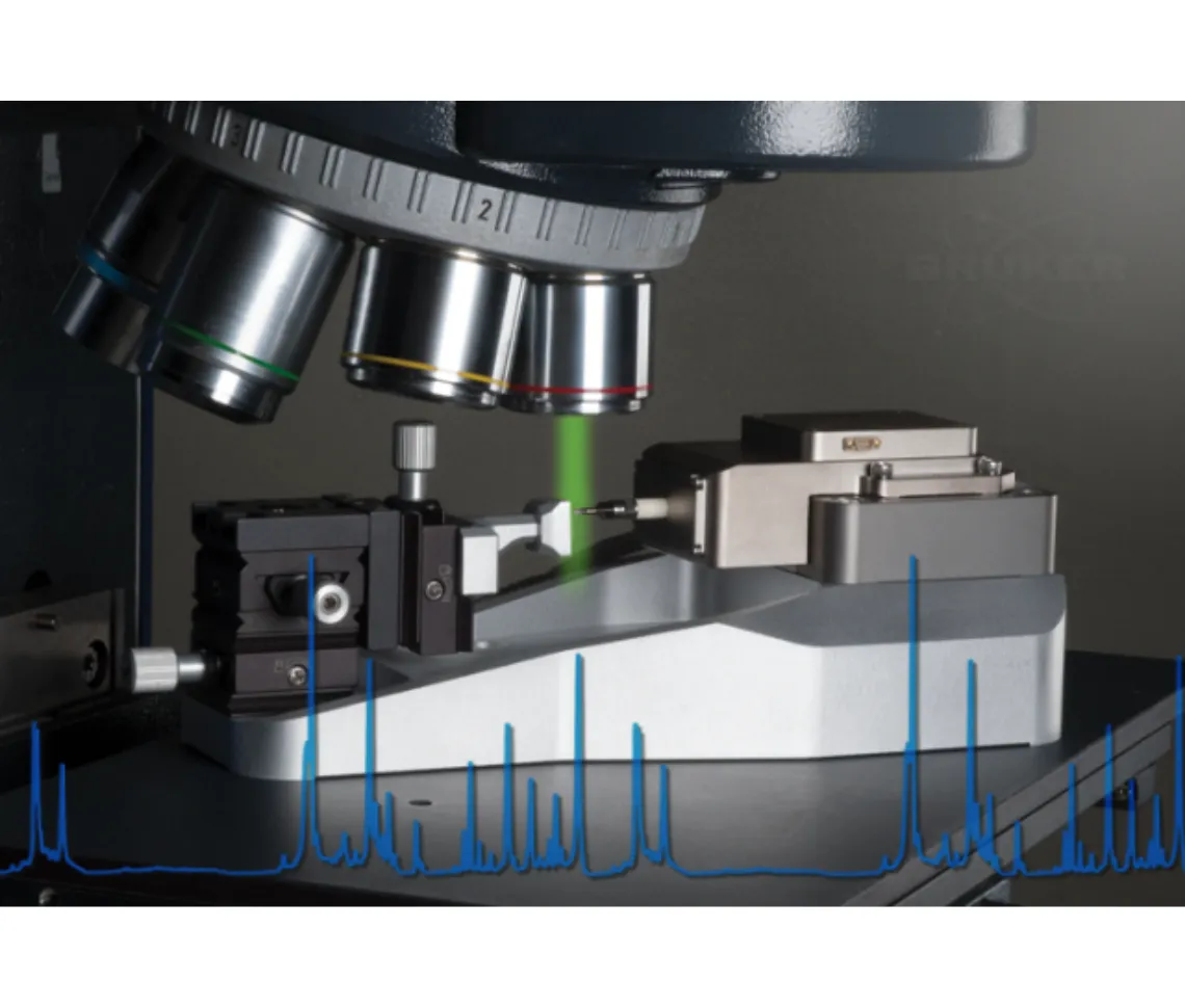
| Optics | Integrated dual-channel tip-centric objective plus offset objective; high resolution with large field of view |
| GUI & Usability | Modern interface; rapid recipe generation; off-tool recipe editing; automated wafer map creation |
| Service & Support | Global technical support; fast problem resolution; local parts depots; customizable coverage programs |
| Roughness Metrology | Sub-angstrom sensitivity; RMS roughness <100 pm; 3σ <10 pm repeatability; <1 min MAM time |
| Depth Metrology | DTMode for trenches/vias from tens of nm to >10 µm depth; <10 s MAM time |
| Sidewall Profiling | CDMode for true CD-AFM; unmatched accuracy; industry’s lowest TMU for SWA/SWR measurement |
| Automatic Defect Review | Automated non-destructive defect review; adhesion data for classification; KLARF-compatible; throughput of tens of defects/hour |
| Surface Profiling | Profile lengths up to 50 mm at 1 mm/s; high planarity; ideal for CMP dishing/erosion, bevel measurement, and step heights |
| Hybrid Bonding | High-resolution bond pad metrology; automated bevel edge inspection; supports advanced hybrid bonding nodes |
| Target Users | Semiconductor fabs, device manufacturers, and metrology engineers |
| Customization | Specifications can be tailored to each fab’s requirements |